2 Describe the Use of Oxide Layers in Semiconductor Industry
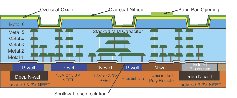
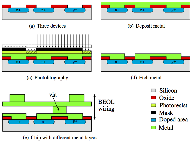
Due to the fast shrinkage of the feature size and the increased number of devices more metal-interconnect layers were required for each new generation of ICs especially for logic chips and microprocessors. Energy gap Eg 8eV.

Sensors Free Full Text P Type Metal Oxide Semiconductor Thin Films Synthesis And Chemical Sensor Applications Html
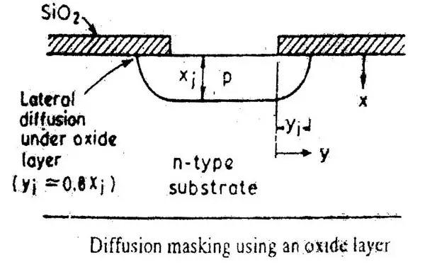
SiO2 acts as a barrier or mask against the diffusion of dopant through the oxide layer.
. The quick build-up of surface topography with the increase of interconnect layers usually results in a poor step-. Oxide layers on semiconductor wafers are etched in a mixture of gases to achieve the proper thickness. Dielectric constant k 39.
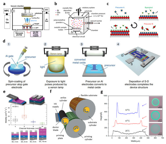
In the semiconductor industry ALD of SiO 2 has applica-tions such as sidewall spacers26 shallow trench isolation liners27 and gate stack liners11 The ALD of SiN x can be used for fabricating sidewall spacers1028 trench liners gate stack encapsulation28 and air gap liners29 SiC is often used as a hard mask layer because of its robust resistance to chem-. There are three methods of embedding thermal oxide into silicone wafer. The interfacial SiO 2 layer may be formed by two mechanisms.
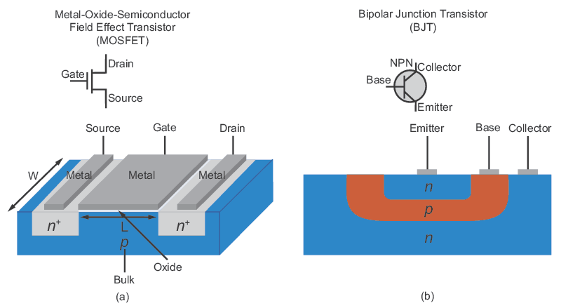
Can be also readily deposited by CVD. Definition of metal-oxide semiconductor. The Metal Oxide Semiconductor as the name itself suggests have a polyGate Oxide layer as dielectric and insulation and semiconductor which constitute the sourcedrain and bulk.
Today it is being driven by the semiconductor. Thermal SiO2 forms smooth low-defect interface with Si. Oxides in semiconductor industry are used for multiple reasons.
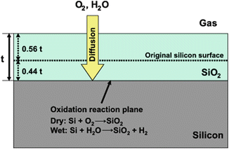
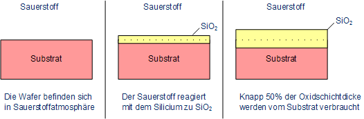
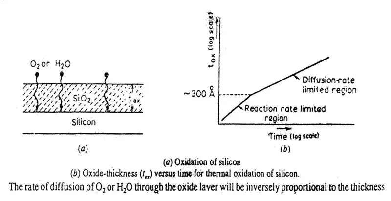
The most simple way to produce silicon oxide layers on silicon is the oxidation of silicon by oxygen. Second W readily forms WS 2 under the same conditions that we use for sulfurizing the gallium oxide layer. Atomic layer etching ALE is a technique for removing thin layers of material using sequential reaction steps that are self-limiting.
The oxide layer is the main factor in determining the surface treatment for a metal surface. SOI MOSFET devices are adapted for use by the computer industry. In semiconductor technology silicon oxide layers are mainly used as dielectrics or latterly also for MEMS micro electro mechanical systems applications.
TiO 2 as a typical species of semiconductor oxide has been widely applied in photocatalysis mesoporous membranes solar cells etc. Native oxide of silicon. Oxides in semiconductor industry are used for multiple reasons.
ALE has been studied in the laboratory for more than 25 years. ALE has been studied in the laboratory for more than 25 years. The most common insulator in semiconductor device technology.
Considering their large specific surface area as well as surfaceinterface effects electrospun TiO 2 nanofibers possess superior performance in. Usually grain boundaries are. A classic example for an oxide-layer-assisted corrosion-resistant alloy is stainless steel in which the alloying element chromium Cr forms an impervious stable oxide layer Cr 2 O 3 also called chromia along the grain boundaries and surface.
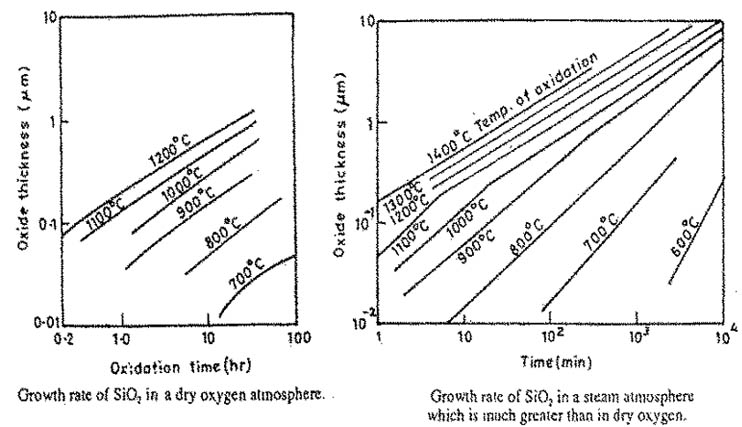
The characteristic of water vapor is that the growth rate is fast but the protective layer is relatively thick and the density is low. See the answer See the answer done loading. SiO2 layer is used as a dielectric between poly Source and drain.
WS 2 is known to act as a hole injector that can be used to overcome the Schottky. Isolation interlayer dielectric scatter oxide ion implantation adaption layers locos technology planarization edge rounding mask layer diffusion alignment marks lithography cover layer to. To avoid the first mechanism oxides that appear to be thermodynamically stable in contact with silicon should be chosen such as Al 2 O 3 and ZrO 2 7.
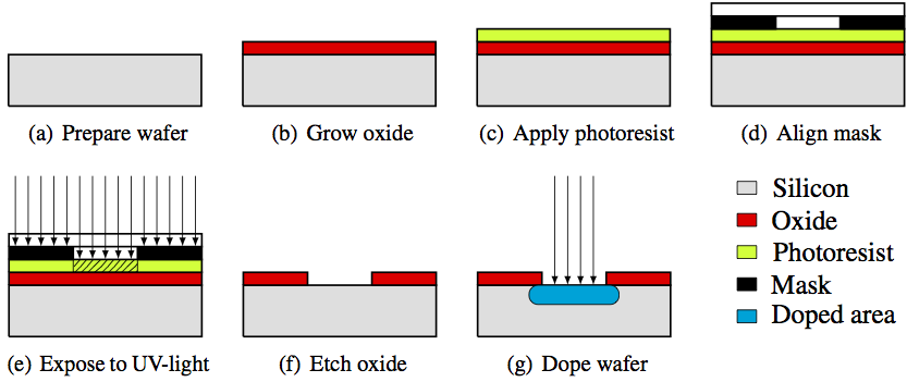
Isolation interlayer dielectric scatter oxide ion implantation adaption layers locos technology planarization edge rounding mask layer diffusion alignment marks lithography cover layer to. In this case oxide is deposited on the silicon wafer. SiO2 is also used in the lithography process as an insulator in the manufacturing process.
The latter requires both oxygen and high solubility. Semiconductor device fabrication is the process used to manufacture semiconductor devices typically the metaloxidesemiconductor MOS devices used in the integrated circuit IC chips such as modern computer processors microcontrollers and memory chips such as NAND flash and DRAM that are present in everyday electrical and electronic devices. The oxide layer is used to mask an underlying silicon surface against a diffusion or ion implantation process.
Dielectric strength 5-15 x 106 Vcm. Formation of silicon oxide layers SiO 2. Chemical Vapor Deposition CVD this is used in the semiconductor industry to produce thin films.
Dopants tend to accumulate near this layer so precautions must be taken during oxidation to prevent this diffusion from occurring. High quality films are obtained by thermal oxidation of silicon. Two different mixtures of gases are being studied to determine whether one.
I a reaction between silicon and the high-permittivity oxide and ii oxidation of the silicon surface during the oxide deposition. The variability in the thickness of these oxide layers is a critical characteristic of the wafer and low variability is desirable for subsequent processing steps. Semiconductors oxides are popular as filler for thermoplastic composites to tune their mechanical properties flexural tensile strength stiffness and hardness for improved applications in biosensors thermoelectric automotive and construction field.
Therefore HF vapor etching is suitable for removing the natural oxide layer of SiNCs. A semiconductor device such as a diode or a capacitor in which a metallic oxide such as silicon dioxide serves as an insulating layer. The former uses pure oxygen to produce a silicon dioxide layer which is slow but the oxide layer is thin and dense.
An SOI MOSFET is a metal-oxide-semiconductor field-effect transistor MOSFET device in which a semiconductor layer such as silicon or germanium is formed on an insulator layer which may be a buried oxide BOX layer formed in a semiconductor substrate. However HF vapor etching can remove only the natural oxide layer without the removal of SiNCs from the substrate. Dopant diffusion is slower through oxide than silicon so the oxide thickness can be monitored to avoid inversion of a lightly-doped substrate.
The oxide layer is patterned by the phtolithographic process to produce regions where there are opening or windows where the oxide has been removal to expose the underlying silicon. Atomic layer etching ALE is a technique for removing thin layers of material using sequential reaction steps that are self-limiting. Today it is being driven by the semiconductor industry as an alternative to continuous etching and is viewed as an essential counterpart to atomic.
Used for the reduction or elimination of the natural oxide layer in the semiconductor industry results in the removal of all SiNCs from the substrate.
Semiconductor Manufacturing
Oxidation Process In Ic Fabrication
Oxidation Of Silicon Springerlink

Oxidation Of Silicon Springerlink

Pdf A Review Of A To Z Of Semiconductor Fabrication

Oxide Growth An Overview Sciencedirect Topics
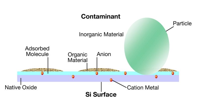
Wafer Surface Cleaning
Fabrication Of Oxide Layers Oxidation Semiconductor Technology From A To Z Halbleiter Org
Semiconductor Manufacturing

Oxide Film An Overview Sciencedirect Topics
1 1 1 Semiconductor Fabrication
Sensors Free Full Text P Type Metal Oxide Semiconductor Thin Films Synthesis And Chemical Sensor Applications Html

Metal Oxide Semiconductor Field Effect Transistor An Overview Sciencedirect Topics

A Thermally Grown 1000 Nm Oxide Layer On Both Sides Of The Silicon Download Scientific Diagram
1 1 1 Semiconductor Fabrication
Oxidation Process In Ic Fabrication
Coatings Free Full Text Recent Advances In Metal Oxide Thin Film Transistors Flexible Stretchable Devices Integrated Circuits Biosensors And Neuromorphic Applications Html

112 Questions With Answers In Silicon Wafer Science Topic
Oxidation Process In Ic Fabrication


Comments
Post a Comment